- Active project
- Electronics
- Git
- Source code
- Windows
Gerber2PDF front end
This is a front-end to the excellent Gerber2PDF command line tool for converting Gerber files to PDF documents.
Downloads
TL;DR: Download it here:
You will need .Net 4.6.1 to run it (although it'll probably compile under earlier versions of .Net - I just can't really be bothered).
Building it yourself
The code is available from my Git repository, https://gitlab.tribbeck.com/windows/g2p-front-end.git.
I used VisualStudio 2017 to compile it.
This code is released under the MIT license.
Copyright (c) 2019 Jason Tribbeck / 7th ARM

Permission is hereby granted, free of charge, to any person obtaining a copy
of this software and associated documentation files (the "Software"), to deal
in the Software without restriction, including without limitation the rights
to use, copy, modify, merge, publish, distribute, sublicense, and/or sell
copies of the Software, and to permit persons to whom the Software is
furnished to do so, subject to the following conditions:

The above copyright notice and this permission notice shall be included in all
copies or substantial portions of the Software.

THE SOFTWARE IS PROVIDED "AS IS", WITHOUT WARRANTY OF ANY KIND, EXPRESS OR
IMPLIED, INCLUDING BUT NOT LIMITED TO THE WARRANTIES OF MERCHANTABILITY,
FITNESS FOR A PARTICULAR PURPOSE AND NONINFRINGEMENT. IN NO EVENT SHALL THE
AUTHORS OR COPYRIGHT HOLDERS BE LIABLE FOR ANY CLAIM, DAMAGES OR OTHER
LIABILITY, WHETHER IN AN ACTION OF CONTRACT, TORT OR OTHERWISE, ARISING FROM,
OUT OF OR IN CONNECTION WITH THE SOFTWARE OR THE USE OR OTHER DEALINGS IN THE
SOFTWARE.
Why did I write it?
While I've documented the way I make PCBs, what I haven't documented is the new way. Or rather, the new application.
I now use Altium Designer instead of Eagle PCB to design PCBs - mainly because of the 3D design (which Eagle now has), but also because of my previous job at InfoVista, where we used Altium.
Altium is really good - although its PDF export doesn't work with my workflow. As a quick recap, using Eagle, I export the PCB as a PDF document, and then import into Xara Designer. I can then arrange multiple PCBs onto the same sheet, and then print them out ready for photo development and etching.
When you initially export PDF with Altium, it will default to an incorrect page size, so you delve into the settings, and find that you need to tweak a couple of things before it'll export as a 1:1 scale. While Acrobat will display it correctly, for some reason it doesn't work when importing into Xara.
After a bit of digging, I came across the Gerber2PDF command line tool, which allows you to convert a Gerber file into a PDF (as if you couldn't guess!).
It has a number of really nice features - the main one being that the PDFs it exports import into Xara very nicely. However, it can be a bit fiddly to remember the incantations used to create the PDFs. So I decided to write a little front end which will call it with the various options.
Gerber2PDF_FrontEnd
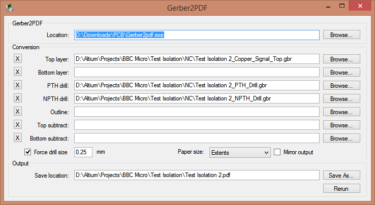
This tool looks like this:

The window is split into three sections.
Gerber2PDF
This is simply the location of the command line Gerber2PDF executable itself. Click on "Browse" to find it - the location is remembered across program executions (as is everything).
Note that all files need to be Gerber files - I use Altium's built-in GerberX2 exporter, so I don't need to convert the Excellon file to a Gerber file. If you have an Excellon format file, you will need to convert this into Gerber using the Drill2Gerber program that is also available from the same place as Gerber2PDF.
Conversion
This is where the input files and configuration is used to create the PDF. Broadly speaking, there are two files used for the top layer, another two for the bottom layer, one for the outline, and two more for drilling.
Each row contains a "X" button, a file location, and a "Browse" button. The "X" button will clear the file location to its right, and the "Browse" button will find the file.
The bottom row contains a number of options.
Force drill size is a check-box that allows you to force the drill size to be a certain diameter. In Eagle, I used a ULP called "drill-aid", which does the same thing. The idea is that you have a small 'hole' in the pad which is the centre of the drill, and when you move the drill down slowly, the drill bit will align itself with the hole - assuming there is a bit of play in the position of the drill. It doesn't help if you are using a CNC drill...
Note that this is only tested with the GerberX2 files produced by Altium.
Paper size allows you to set the PDF paper size. Options are "Extents", "A4", "A3" and "Letter".
Mirror output allows you to mirror the layers. Since this is designed to print onto the side of an acetate sheet which is placed against the board, the layers will be correctly mirrored for that (it is assumed that they are printed as if viewed from the top of the board, so the bottom layers will actually be mirrored).
Output
This is where to save the file. Rerun allows you to simply rerun with new options without having to specify a new save filename.
Using it
The way the program outputs the PDF is as follows:
- The top layer is printed in black on the first page
- The outline is printed in black on the first page
- The PTH drill is printed in white over the first page
- The NPTH drill is printed in white over the first page
- The top subtract layer is printed on white over the first page
- The bottom layer is printed in black on the second page
- The outline is printed in black on the second page
- The PTH drill is printed in white over the second page
- The NPTH drill is printed in white over the second page
- The bottom subtract layer is printed on white over the second page
If you do not specify a top layer, then the first page is skipped, and you only end up with the bottom layer on page 1. Conversely, if you do not specify a bottom layer, then the second page is skipped.
If a Gerber file is not specified for one of the options, then it is not printed.
What is the use of the subtract layers?
These can be used to add inverse text to copper areas - for example, I often stick a logo in a large expanse of copper pour. I normally do this as a union that I've copied between projects, but if you want some text, then Altium's options are a little bit lacking. You can do some text which is inverted, but that will not merge into the copper pour (it sees it as a different net, so will leave a gap). This option allows you to specify a layer in Altium into which you can put such text, and then it'll be plotted in white. Note that this will not be reflected in any design rules, so if you accidentally erase a line that is important then you won't be told...
Examples
Here are some examples.
Test Isolation 2
A top-layer only one which I was using to test isolation routing, although it ended up as a test for my new printer for photographic board making!
Note that this one was created using the options above. There are four holes in the board - the two surrounding the 7th ARM logo in the middle, and two at the bottom. These are demonstrating the "Force drill size" option - the hole in the middle is 0.25mm for each of these holes, allowing the drill to 'lock in' to the location.
Eprom emulator (ISP ROM Prototype)
This is a top and bottom layer board - the top layer won't be used for etching, but as a reminder of where any wire jumpers need to go.
Note that this was designed before I added the "subtract" layers, so I would've done the copyright on the top left of the mirrored bottom layer.
Also note that this one uses the outline layer (which I use "Mechanical 32") to add the outline.
If you want to have a go with this, then here are the Gerber files.

Although if you make it yourself, then good luck, as I've not given any information as to what chips do what :)
