- Eagle PCB
- Electronics
How I make PCBs
There are many web sites talking about how to make PCBs - however, I thought I'd do one myself, as I create the films in a slightly different way.
PCB design
I use Eagle PCB to create PCBs. I have bought the professional version of Layout and Schematic for MacOS so I can make large boards (I don't rate any auto-routers, so I didn't go for it).
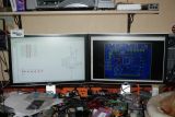
This board is one I'm working on for the second version of a 2.5D CNC miling machne I'm about to start work on.
Creating the film
With the board designed, I set up Eagle to display the primary layers (bottom, pads, vias, dimensions and holes), and tell it to print - however, instead of printing direct to the printer, I print to a PDF.
This is because there's a problem with Eagle's direct print output where it prints holes slightly offset. It also gives me the opportunity to import it into Xara Xtreme (which runs on a VM on the Mac) and join several PCBs to etch at the same time. If I do this, then I will also put some text on the PCB.
This then gets exported as a high-res PDF/X document, and then on the Mac into the standard Preview.
I then print it using an HP Deskjet 1220c printer (which can do A3) onto an ordinary inkjet compatible OHP sheet. I have a special setting called "PCB" which prints in black and white at as high a resolution as possible.
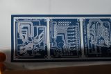
This picture shows three PCBs, the left one has a 0.5mm pin spacing PIC on it (unfortunately, the picture's a bit blurred because it was difficult to hold steady).
The important thing to note is that it is not opaque. I tried to show this by having some background showing through the "black" design.
Exposing the PCB
I bought a UV exposure unit about 10 years ago - it still works, although it's only single-sided, and has problems towards the extremeties of the area.
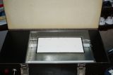
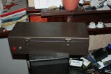
I cut the board to the rough size of the board to be etched, and file the edges - if there's raised bits, then the edges can become blurred.
For the board I use, 5 minutes in the exposure tank is required (I've got a thinner board I sometimes use which needs 4 minutes). If I need to do a large board, then I'll extend this to 6.
Developing the PCB
After that time, the board has been exposed.
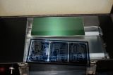
You can just make out the bits that are greener that have not been exposed.
It then gets dipped into developing fluid - this is about the largest I can do in this ice-cream container. I do have a larger tray for bigger boards if necessary.
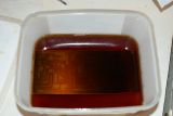
Once the developed sections are developed, then the board looks like this:
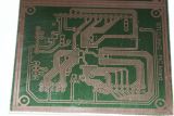
The tracks coming away from the middle chip (PIC) are 0.01" thick - I have done tracks half this width successfully, but this is the thinnest I feel comfortable with.
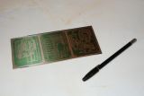
Finally, I make a visual inspection, and using an etch-proof pen, I fill in any gaps or things I don't like:
Etching the PCB
I used to do this manually, in another ice-cream container, but late last year I bought an etch tank, and also fitted a sink to my "shed" (it's actually the out-house).
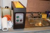
This takes a variable amount of time depending on the size of any empty areas that need etching - this one took about 7 minutes; this is about 3/4 through:
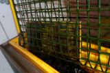
And when competed, washed and cleaned:
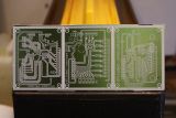
At this point in time, I do a visual inspection and clean up any tracks that have been joined - this can happen if there was dirt on the film or board, or if my earlier repair was a bit too aggressive. This has a couple of bits that need tidying.
Drilling
I use an old pillar drill for making the holes - and plenty of light around it.

I have a number of drill bits for making PCBs:
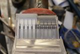
From left to right, they are: 0.6mm, 3x0.8mm, 1.0mm milling bit, 1.0mm, 2x1.3mm 2x1.6mm. I also keep some spares of the smaller sizes elsewhere, as well as a 2.4mm milling bit. Furthermore I have some non-tungsten carbide drill bits from 2mm upwards.
After drilling 0.6, 0.8 and 1.0mm:
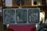
The middle board has some holes that need elongating (power supply socket); this is why I have a 1.0mm milling bit, since I use these sockets frequently.
And after drilling all of them:
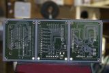
Cutting the board
With everything drilled, the board needs cutting. I use a vice which can be rotated around its axis. This allows me to use a saw with ease:
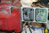
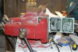
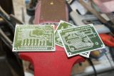
I then file the edges down (I have three grades of files depending on the size and thickness of board being made). In the above picture, the left has been filed.
Tinning the board
I like tinning the board - it makes them last much longer, especially in some of the harsher environments some of my boards find their way in.
I remove the UV developer coating using some thinners:
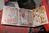
Because the tin-plating I use likes a nice and clean board, I use a PCB etch block to remove any surface crud that has remained (you can use this instead of thinners, but it's a lot of work).
On the left is a board that has been cleaned in this way; on the right is one that needs cleaning:
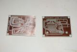
With all three boards cleaned:
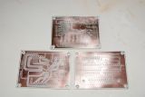
I then put the boards into the tinning fluid - this is after about 30 seconds:
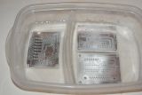
With a fresh batch of tinning fluid (which lasts about 6 months), I leave it for about an hour at minimum; later on, I'll leave it for 3 hours.
After a couple of hours, they look like:
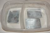
And subsequently washed:
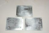
And that's how I make PCBs. There are other ways that it can be done, but this works for me.
