- Electronics
How I make two layer PCBs
Just a continuation of my "how I make PCBs" note, this is how I make two layer PCBs. The PCB design is the same - it's just the developing, etching and drilling that are different.
There are other ways to do this - but I'm limited by only having a single sided UV exposure box. I also can't do plated through hole (PTH), so this means that any holes need to be plugged with a wire, and soldered on both sides. For large areas of copper (such as ground planes), this can be quite difficult as the heat needs to get to both sides. Sometimes I'll enable thermals for Vias in Eagle.
The basic technique
I call this technique OSAAT - One Side At A Time, and that pretty much describes it.
I cut the board to be oversized at one edge, so I can stick the OHP sheet to prevent movement (although if it's reasonably freshly printed, it'll have some stickiness from the ink).
So, one side has its protective label on, and the other has the transparency on it.
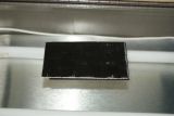
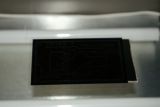
This is a memory interface for a project I've not announced. It's called XilinxTracker here, but has changed name a couple of times since then...
Exposing (1)
I remove the transparency film, but leave the protective tape on the other side. It then goes through its first exposure, an after developing:
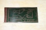
This is the bottom side of the board. I use a pen to tidy up the areas that don't need to be etched (similar to the visual inspection - except I cover the bits that weren't convered by tape).
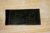
Etching (1)
Again, leaving the protective tape on the other side, I etch the board.
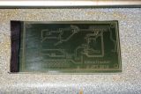
Drilling (1)
In order to align both sides, I drill a number of holes on the board, preferably one in each corner. For this board, there's 4 screw holes - mostly near a corner - so I use those, plus one of the vias.
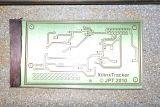
It's difficult to see, but there's one via drilled towards the bottom left of the board.
Alignment
This is the most difficult stage of the operation, and I tend to do this at night. You need to get the other transparency perfectly aligned with the holes that you've drilled.
This certainly isn't easy, and this took a good 10 minutes of shuffling the transparency around (not easy when it's a little sticky, and when you don't want to smudge it).
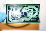
Exposure (2)
Once it's in the right place, if it's a bit sticky then it helps as it won't move around too much. After going through the UV box and developer again:
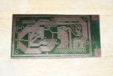
Etching (2)
On the etched side, I now run the etch-proof pen over the surface. You need to make absolutely sure that everything is nicely covered.
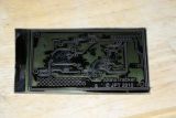
And then in the etch tank it goes again.
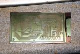
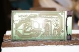
Drilling (2)
The rest of the holes can be drilled from either side.
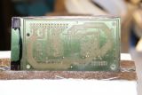
It's very difficult to get a 100% accurate alignment. You can see some of holes not quite in the centre on the other side. Well, most of them in fact!
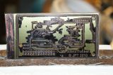
This doesn't actually matter unless they're really bad.
Finishing off
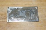
After cleaning the etch resist off it, and filing the sides:
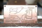
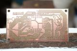
Tinning it is the same as for single sided boards - except both sides get done:
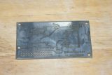
Populating
Because the holes don't conduct electricity, you need to solder wires that join both sides. This is very time consuming, but it's worth it. I keep 0.6mm and 0.8mm bare wire for this purpose - although sometimes the remains of an LED leg will be used!
When it's populated, you won't tell that the holes aren't exactly in the right place:
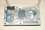
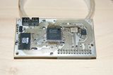
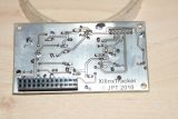
One day I'll invest in a CNC drill - then I'll drill all the holes before etching any of them. Hopefully that'll give me better alignment.
