- Electronics
Prototype modifications
There have been a number of modifications made to the original prototype PCB, in order to get it working.

The original board was designed in a bit of a rush - I had a friend coming to visit and I wanted to show him. Unfortunately, he didn't make it in the end, so the rush job didn't need to be done.
Mod 1: Reset switch
I'd neglected to add a manual reset switch. This meant it could only be reset via the JTAG interface.
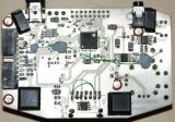
This is the long green wire that stretches the width of the board. I drilled additional holes on the right (as you look at it) for a small Omron switch (I've got a number of them kicking around).
Mod 2: Pull-up resistor for reset
I'd also forgotten to put a pull-up resistor for the reset.
This is the non-SMT resistor to the left of the board, soldered to the JTAG connector.
Mod 3: Audio master clock
I'd been basing the audio DAC interface from an Atmel application note - however, the DAC they were using I couldn't find in Farnell or RS, so I used a different one. What I didn't realise was that the PLL divider/multiplier would be difficult to get right in order to make the SCLK an exact divisor of the 18.432MHz input clock.
The modification was to use the PCLK2 output from one of the pins as the MCLK pin for the DAC. This is derived from the master clock in the CPU.
This is the wire that comes off the bottom of the ARM to the 8-pin chip to the right.
Mod 4: FRAM chip
In the earlier prototype, I had space for an SD-Card interface. However, I needed somewhere to store the high scores. A 1GB SD-Card would be a bit of an overkill, so I removed the socket and replaced it with a PCB that was similarly arranged to take a EEPROM chip.
In a moment of lunacy, I ordered the wrong EEPROM, and, being a late Friday night, I hunted around for other SPI interfaces. Luckily I had a 32K FRAM device in my collection - which has an identical pin-out to EEPROM.
This is the extra PCB soldered at the bottom of the board, with the 8-pin chip on it.
Mod 5: MISO/MOSI pins
I'd got the two pins confused on the FRAM interface board.
This is the two wires connecting the FRAM board to the CPU board (about middle bottom).
Mod 6: MISO pin (from CPU)
I didn't have the Atmel device in my PCB design, so I created it manually. Unfortunately, I got a bit carried away, and labelled the PA24 pin with PA12's supplementary details. When I went to wire the MISO pin, I looked for the nearest MISO to PA13 - which happens to be next to PA24. So what was the MISO pin wasn't, and I needed to wire in a new one.
This is the green wire coming off the ARM chip to the right.
Not a modification, but a note
You may see that there are two unpopulated pads to the top left - underneath the USB connector (there are actually 3).
These have been left unpopulated as I don't need the USB interface yet (although it would be nice to take screenshots).
I'd need to implement some form of USB stack on the device, and that can wait...
