- Eagle PCB
- Electronics
- Xilinx
The board
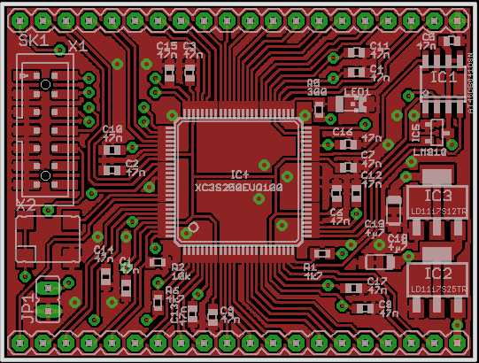
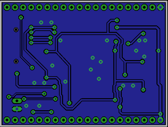
The PCB layout is as follows:
Top

Bottom

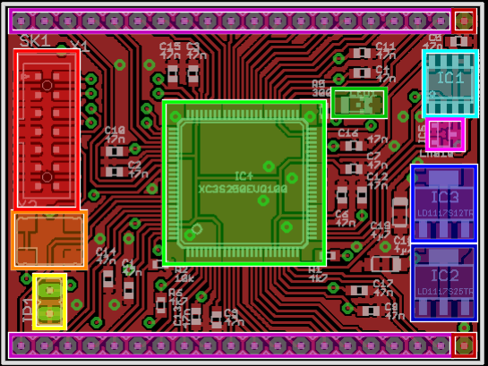
Component positioning

The various sections are colour-coded (starting top-left, spiralling clockwise):
- 19 I/O pins, 0.1" spacing
- Ground
- 2Mbit configuration FLASH ROM (AT45DB021D)
- Reset generator
- 1.2V voltage regulator (LD1117S12TR)
- 2.5V voltage regulator (LD1117S25CTR)
- Single 3.3V power supply
- 19 I/O pins, 0.1" spacing
- PROGB pins (to allow a form of reset)
- 50MHz oscillator
- Xilinx 14-pin JTAG (2mm, suitable for Platform Cable USB II)
- Xilinx XC3250E-VQFP100 device
- DONE indicator (LED)
The PCB is a two-layer board, and no components are on the underside. There is the possibility to make it single layer, but you would need to solder two wires into the same hole (which is doable with wire-wrap wire).
Components
All of the 47nF capacitors and resistors are 0603 size, which is the smallest size I've done. There probably won't be much of a reduction if I went to 0402.
The LED is a 1206 size device. I do have some 0805 size LEDs, but there's space for 1206.
Traces
Most of the traces are 10mil. All but one of the power traces are 24mil (the one that isn't is 10mil, and that only powers the crystal). All traces going to the FPGA are 10mil. Some of the underside signal traces are 24mil as well (mainly due to laziness).
Holes
The 40-main holes and two for the PROGB connector are 1.0mm, whilst all the via holes are 0.6mm, drilled using a fairly large bench drill.
In order to allow a slight amount of inaccurate positioning of the PCB film, the vias are 45mil octagons. This allows a 10mil trace to go around it with a 125mil grid. I prefer to use octagons to square and round pads because square ones don't allow traces to go around them as nicely, and round pads have slightly smaller footprint (so less area).
The five vias inside the FPGA area aren't drilled, but will be if this board is made by a proper PCB production facility. All of the ground wires are connected except for two without the bottom layer anyway (I only needed to connect two of the ground vias). Those five vias are purely used to prevent local fluctuations in the ground signal (and one of them is used to denote the chip orientation - hence its proximity to the dot).
Ground plane
Both sides of the board have a solid ground plane. This is constructed of 10mil wires and a 12mil isolation. Orphans are initially disabed during design, but are enabled upon completion.
DRC rules
The PCB completely fulfils my DRC (Design Rule Checks) for the PCB production I can do at home, with one exception - C5 (top-right) bounds interferes with the bounds for IC1. I have approved this rule because the 0603 package has quite wide bounds (which is useful to know when holding them with the tweezers I have), but the orientation of IC1 is such that the bounds don't interfere with the legs of the chip itself.
Note that if you use the built-in Eagle DRC rules, then they will fail on the spacing between the pins on IC4. I did a lot of experimentation in what I could achieve with my method of creating PCBs.
